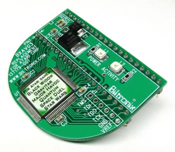
In 1982, there were six color vector arcade games released by Atari that included on the game board Atari's own custom IC #137179-001. The games were Black Widow, Gravitar, Major Havoc, Quantum, Space Duel, and Star Wars.
The BXAVG module is a direct plug-in logic replacement for the original Atari IC chip. The BXAVG has been tested and works 100% correctly in all 6 of the Atari AVG games that include...
Black Widow, Gravitar, Major Havoc, Quantum, Space Duel, Star Wars
The Atari custom chip 137179-001 is a 40 pin DIP package that works within the section of the game board comprising the VSM (vector state machine) and has been commonly referred to as the AVG (analog vector generator). The custom chip contains a relatively large amount of logic that replaces several smaller standard TTL chips (approximately 14 altogether) with a single part. I suspect that this was done as a cost saving measure.
Since 1982, the Atari AVG chips have been failing at what seems to be an ever increasing rate. It has become extremely common to see non-working game boards for sale on eBay (and other popular sales forums) that are already missing their AVG chips. Personally, I have seen as many boards missing the AVG chip as those missing EPROM, MPU, and POKEY chips. Odds are actually pretty good these days that a so-called 'untested' board just needs a new AVG chip. As far as I know, nobody has definitively determined the root cause or common causes of failure in the original Atari AVG chips. This being the case, even NOS (new old stock) or chips with low mileage cannot be comfortably relied upon.
Most proud owners of AVG chip dependent games now assume that the failure of the AVG chip in their games is evitable or at least very likely to occur well before any other sort of catastrophic failure that could end the useful life of their game. To ward off disaster, owners of these games typically keep spare AVG's in their stockpile of parts. Such spare AVG's can be original Atari chips (that for some unknown reason still work) or a third party functional replacement such as the BXAVG module.
How It Works (Not too technical):
Detailed study of the circuitry used in previously released games such as Tempest and Battlezone reveal the bulk of the internal organs of the AVG custom IC. The schematics of the six games in which the AVG chip is used reveal that the circuitry of the previous games was simply expanded with respect to 'bit width' by a couple of bits. Since almost all of the standard TTL chips were built to support 4 bits each, then adding another bit or two would still require adding fully loaded standard TTL chips ending up with half of each additional chip not being implemented for anything. A group of many TTL chips (let's say 14 of them averaging 16 pins each) requires a lot of real estate (large PCB area), a lot of drilled holes (more than 250), a decoupling capacitor for each chip, and a lot of printed circuit connections (PCB routing) between all of the chips. At some point, the cost of adding more standard logic chips exceeds the cost of the much smaller custom IC. I believe that the new games had reached this threshold and that's why Atari created the AVG chip.
The AVG chip is essentially a fancy 14 bit counter (referred to as the 'address controller' of the VSM), the output of which is used to address vector ROM and vector RAM. The auto-incrementing function of the counter helps to automate the very complex task of drawing vectors on the monitor. In this way, much of the burden of drawing vectors is removed from the main microprocessor. What makes this counter special is that its value can be saved to a 3-level internal stack memory and it can also be loaded from that same memory. It can also be loaded from an input port that receives data from vector data shifters which decode and modify data that they get from vector ROM or RAM or the main microprocessor. Since the output of the AVG counter (which is an address) can directed back to the beginning of the VSM, it becomes a little more obvious that a logical loop exists. I suspect that this loop enables the system to easily repeat vector drawing tasks quickly and as for as many times is needed without requiring an excessive amount of work from the main microprocessor. This provides the microprocessor with more time to work on other tasks such as running the game logic (ship movement, collision detection, generation of sounds, calculation of scores, etc.).
Presently, there are just two main types of AVG replacements, TTL boards with several standard logic chips and single chip boards that have a single CPLD (complex programmable logic device) chip.
Which Type of AVG Replacement Is Better?
Reliability:
Typically, AVG replacements comprised entirely of TTL chips are considered favorable because they are repairable by the average end user who has moderate electronics skills. To counter this, some have argued that single chip CPLD solutions offer very high reliability due to the significantly lower component count and connection count (fewer pins to interconnect). The point here supposedly being that they are less likely to require repair in the first place than a multi-chip TTL solution.
I think it is important to keep in mind that the so-called 'higher reliability' of the CPLD board is moot. The point is whether or not a board can be repaired right? Some would say that the CPLD module cannot be repaired by the end user, however, this is only true if a new chip is not available. After all, the chip is socketed so it can be easily replaced. As far as I know, replacement CPLD chips are still available from the original people who created their specific model. It is also likely that in the future someone will either write and publicly release working CPLD code or one of the people who has already produced a CPLD board will release their code. Either way, any end user who has access to a JTAG programmer can flash a new CPLD chip and thereby repair the board. All they need to start with is a good blank chip which are certainly available.
Physical Appearance:
The most obvious advantage of the CPLD modules is their much smaller board size relative to the TTL boards. Do you prefer the 'old school' look of the TTL board when it is mounted on your game board? Maybe you couldn't care less just so long as it works. Maybe you will prefer the smaller the CPLD board.
Accuracy of the Replacement Logic of AVG's in General:
TTL multi-chip boards and single-chip CPLD modules have equal ability to emulate the original AVG chip accurately. However, I want to state simply that it is my opinion that most of the AVG replacements produced to date, regardless of type, do not. If any module doesn't perform perfectly in all 6 of the AVG games then that is proof that something is not quite right.
I do believe that my new BXAVG does work 100% correctly. I believe this is true based on the fact that I have addressed all of what I believe to be the common sources of errors that others have fallen prey to and because I have tested my BXAVG in all six of the AVG games and have found no issues of any sort. I have tested a couple of boards made by others and discovered errors. I was able to reprogram one such board that showed errors on some games with my own code and thereby eliminate those errors.
An advantage of the CPLD module is that the functionality can be programmed to mimic the original Atari AVG custom IC precisely whereas most of the existing TTL based boards cannot (I gonna catch hell for this statement but I can back it up with proof).
I know that some people will argue with me to the death on this issue. I won't allow myself to be drawn into long debates (I'm entitled to my opinion just as you are) but I will present my own arguments here. Agree with me or not, decide for yourself.
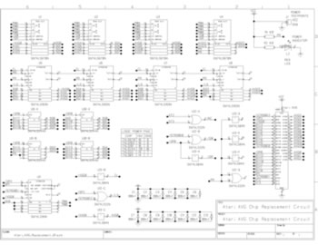
This discussion requires a little more history. Back in 2001, Jed Margolin released into the public domain a schematic drawing along with a verbal description intended to represent the functionality of the AVG section of a new game that he had worked on (Tomcat) but was never released. He did not claim that it represented exactly what was inside the original Atari AVG chip used in the first 6 games. There are some functional differences. For obvious reasons, the schematic became popular among arcade enthusiasts because it apparently gave them all of the information required to actually build a working circuit that could possibly replace the AVG chip. Since then, a number of TTL circuit boards based entirely on this schematic have been produced. Some of these I have listed in a following section below.
Before I continue, I want to say that any statements that I make with respect to Jed's schematic are made with total objectivity and are not intended to be critical of Jed personally or his skills in any way whatsoever. I greatly appreciate Jed's long history of excellent contributions to the world of arcade enthusiasts and have great respect for anyone who makes an effort to provide everyone with useful practical information that can be used to help preserve our classic games and to provide insight towards developing improvements and repair solutions. I personally have learned a great deal over the years by reading Jed's many documents.
The only TTL board that I have seen that works 100% correctly in all games is Clay Cowgill's board. Why is Clay's board different? Clay's board was produced prior to the release of Jed's schematic and has a PAL chip that replaces certain logic from Jed's schematic. I believe that within the PAL chip lies the logical functional difference and the reason for why Clay's board works properly and others based on Jed's schematic do not. Put simply, Clay performed his own research and got it correct. Those that followed Jed's schematic to the last pin have some slight issues, that is if you call occasional errant vectors a slight issue. The games will all play regardless and that's better than nothing despite a few brief graphical errors.
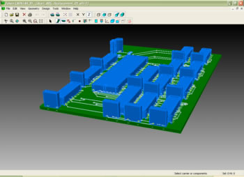
Just after I started into the arcade hobby several years ago, I myself discovered Jed's schematic online and immediately considered making my own TTL PCB. I redrew the entire schematic within my applicable software package and routed a PCB as shown below. The 3D model doesn't show fully rendered component models, but you get the idea. I never actually built this one. Why not? Read on...
Claims have been made all over the internet that some of the TTL boards released between 2001 and the present only appear to work properly in certain games. I have little of my own experience to verify this but I have friends in the hobby and on forums that verify that this problem exists. There does appear to be some inconsistency as to which games have problems and very little specific information on exactly what those problems are (as in how do they manifest themselves on the monitor).
I thought it was a relatively safe bet that the majority of the TTL boards that have been available up until now have been based entirely on the Jed Margolin schematic. Because of the aforementioned issues with some AVG replacements, I had become concerned that the schematic was not entirely accurate.
I decided to build the CPLD type of board mainly because I was keen to learn how to program CPLD devices using VHDL. I also knew that it would simplify assembly of the boards. Another big advantage is that the CPLD approach provides me with a way to arbitrarily change the functional logic using code. This is a great way to experiment and fix problems without having to redesign or hack a PCB. Since I had my doubts about Jed's schematic, I felt that the CPLD was the only sensible option.
I went ahead and designed the BXAVG board and built several of them. I wrote the VHDL code to precisely mimic the logic of Jed's schematic. I flashed the first BXAVG and tried it out in my custom homemade AVG tester box. It passed on the first attempt... or did it?
I was so excited at this apparent success, I couldn't wait to try the new module in my Space Duel. It seemed to work great. I was truly thrilled. After a few minutes playing Space Duel, I noticed a slight error. Whenever anything exploded, there was a fireworks display, a pattern of dots moving away from each other. Near the end of the fireworks display sequence, a short line would suddenly join two of the dots and then just quickly vanish. This happened on every single explosion so when things got busy, it happened frequently enough to become a bit annoying. This was obviously a logical error of the VHDL code in the CPLD. Needless to say, the original AVG chip didn't ever show this error.
Upon further study of Jed's documentation, I soon realized that proof of a discrepancy in the schematic was right under my nose all along. The verbal description provided by Jed along with the schematic specifically describes the behavior of the AVG0 output, how it is set, how it is cleared, what else it does when it is set, and why it is inverted with respect to the other AVG output bits. Do these descriptions match the functionality of the schematic? They absolutely do not.
Discrepancies between Jed's schematic and actual AVG functionality:
- The schematic indicates that the AVG0 output is simply the inverted output of the least significant bit of the 14 bit counter output. It is not. AVG0 is a separate entity and it has its own behavior. Specifically, AVG0 is generated by a separate 'D' Flip-Flop.
- The schematic indicates that AVG0 is saved to and read from the stack memory along with the other AVG counter bits. It is not. AVG0 is always set whenever a value is popped from the stack, when the input port is read, or when the AVG chip is reset.
- The schematic indicates that all 14 of the AVG outputs 'count' on the rising edge of signal ST3 so long as signal ST2 is low. They do not. Only AVG0 does. The other AVG outputs, comprised of a 13 bit counter will count on the rising edge of AVG0.
- The schematic indicates that AVG0 will 'count' (meaning toggle) and conditionally increment the higher order AVG output counter bits 1:13 on the rising edge of signal ST3 so long as signal ST2 is low. This is actually true but there is a another condition that Jed's schematic does not accommodate. Jed's schematic indicates that AVG0 cannot 'count' (meaning change state) while signal ST2 is high. This is false. The state of AVG0 can in fact change while ST2 is high. I have captured logic analyzer data to prove it. In an Atari AVG chip, the rising edge of signal ST3 will always change the state of the AVG0 output from low to high (and thus increment counter bits AVG1:13) regardless of the state of signal ST2. While ST2 is high, AVG0 will not change back to the low state on the rising edge of signal ST3.
Further to the above, if the relevant details of the Tempest and Battlezone schematics are studied, one can see exactly how the AVG0 output actually works and that it agrees with the above mentioned issues. If one assumes that the Atari AVG chip is an exact logic replacement that simply includes a 1 bit increase in word width (from 13 to 14), then the entire functionality of the Atari AVG becomes completely obvious, to wit, it does not match Jed's schematic in several respects.
Soon after discovering the above issues, I was able to modify my VHDL code to fix them all and I finally ended up with a fully functional 100% AVG compatible logic replacement.
TTL AVG Replacement Boards: An easy hack to improve performance:
If you have a multi-chip TTL board that is 100% true to Jed Margolin's 2001 schematic, you may have discovered that it causes some graphical errors on certain AVG games. The root causes, as described above, can be fixed by performing simple hacks to the board. By cutting a few traces and adding a few small jumper wires, you can employ existing unused gates to fix a couple of the functional inaccuracies with respect to a real AVG chip. You can download the marked up schematic below.
With respect to issue #4 above, ideally, as in the original AVG chip, AVG0 would be generated by a 'D' Flip-Flip. There isn't one available on the TTL boards based on Jed's schematic, but the missing condition for setting AVG0 (logic high represents value 0 on this output only) on the rising edge of ST3 regardless of ST2 can still be met.
Also, issue #2 can be fixed. This isn't really absolutely required so it's an optional hack, but it does make the circuit more true to an original Atari AVG chip. Since the /AVG0 signal is always stored to the stack memory (and therefore always popped) as a logic zero, there's no point to saving it and popping it at all. The hack allows the loading function of the 74LS193 counter to load zero for /AVG0 directly rather than through the stack or the buffer. You can see now that the stack is actually only required to handle 13 bits, not 14. If it wasn't for that 13'th bit of storage, one of the 74LS670 chips could be eliminated. The AVG0 stack storage hack can be done but ultimately it won't change the performance at all. On the TTL board, this hack almost isn't worth the effort to perform. It just eliminates a single line of inputs and outputs that could eventually fail. Less points of potential failure equals higher reliability. The stack hack is mainly educational in nature. It demonstrates simply how to eliminate 1 bit of word width from the storage capacity requirement. In a CPLD implementation, this hack is very relevant because it directly results in saving some valuable chip resources. However, if someone wants to route a new TTL board, it would obviously be wise to include all of the markup changes.
I have marked up the original schematic to show the connection changes. I'm not going to hold your hand by providing a bunch of pictures that show every single trace cut and added connection. Obviously, there are several models of TTL boards and all are routed differently. Besides, I do not have any of them in-hand with which to work. You will have to determine for yourself the best places to cut traces and solder new jumper wires. If anyone performs this hack on their board and it works and if this person would like me to post their photos of the work, I will do so if requested.
Jed's AVG Replacement Schematic with Fixes: Download PDF File
Note 1: If you print the marked up schematic and the markups do not print, change the print options in the print dialog to include "document and markups".
Note 2: The AVG0 counter hack cannot be performed on Clay's board nor is it required anyway. The PAL chip on Clay's board already handles things correctly.
Over the years, there have been several AVG replacements made available by arcade enthusiasts. Sorry, I haven't provided source/purchase links to these. Possibly not all of them still have links but you can Google them if you're so inclined. Some of these have been reported as having issues with certain games. Issues can be as benign as simply not having been tested in a specific game or as serious as causing graphical errors that are visible to the player.
Here's a short list of AVG replacements made by other people (in no specific order):
- 1999 - Clay Cowgill's TTL Board AVG replacement (Pic1)
- This board is comprised mainly of standard TTL chips but it does have one small PAL chip that is custom programmed to replace a few standard TTL chips in order to reduce component count.
- It is my personal opinion that this is the only existing TTL board that works 100% correctly.
- LeopardCats TTL board AVG replacement (Pic1, Pic2)
- JROK prototype Xilinx single chip AVG replacement (never released?)(Pic1).
- 2005 - Cinelabs Xilinx single chip AVG replacement by Omar Vega (Pic1, Pic2)
- Used to be sold at Arcadeshop $35 Description, Special note: Site claimed Space Duel not supported and not tested in Black Widow, Gravitar, Quantum. Site claims tested and working in Major Havoc and Star Wars.
- I have tested one of these in my Space Duel and found no issues.
- I have tested this unit in Black Widow and there were occasionally stray vectors appearing. This did not effect game play and did not occur often but I noticed them from time to time, maybe 5 times in 10 minutes of play.
- There is an LED on the board that is hardwired to the AVG0 output. My concern regarding this LED is that the series resistor for it is only 82 ohms (on my sample). This is too low a value in my opinion. Normally, the outputs of the chip rise to 5V, however, due to the excessive LED current that the AVG0 is attempting to supply, the output voltage drops to just 3V. I suspect that some boards may see this signal drop even further and this may lead to noise problems or even logical errors occuring intermittently on some games. The fix is obvious, either increase the resistor value to something reasonable (220 ohms) or remove the LED or its resistor entirely.
- I can reflash this Xilinx board for you with my own code making it compatible with all 6 games. When I do this, I typically also cut the LED traces and jumper the LED to a previously unused output on the chip so that it will flash the same way as the LED on the BXAVG. Unloading the AVG0 output in this way allows it to reach the full 5V level and thus reduces the game's sensitivity to noise and/or errors. I also change the resistor to 220 ohms.
- Mark Spaethe - TTL Board AVG replacement (Pic1, Pic2)
- This board was supplied with several of the 2011 reproduction Quantum boards (by KLOV member Tronic).
- 2012 - JROK new version Xilinx single chip AVG replacement, sold at Arcadeshop.
- I've heard that these work well. This product came out a few months after I released the first BXAVG and posted the info about it on my site.
My opinion on Activity LED function:
Some of the AVG replacement boards produced to date have a power LED on them. Some boards also have an additional LED that is supposed to indicate some sort of functionality. The only problem with their activity indicator LED's (in my opinion only) is that they are directly controlled by AVG signals that are toggling at rates far too fast for the human eye to distinguish. Written descriptions of their operation include phrases such as "the LED will appear dim" on a certain game and maybe a bit brighter on another game. When things lock up, the LED would appear very bright or stay completely off. I find the whole discussion of LED brightness a bit ambiguous. After all, what exactly does dim or bright really look like to an individual without context? Granted, with some experience, one would get to know what it normally looks like but I would prefer a display that is more obviously determinate regardless of the individual's experience (or lack thereof) with it.
The BXAVG also includes the same sort of LED's, however, the 'Activity' LED always blinks at a rate that makes it very easy for you to see it flashing. It also blinks at a 50% duty cycle so that when it's on, it's bright, and when it's off, it's completely off. In other words, if the LED ever stops flashing, whether it locks up in the on state or the off state is completely irrelevant (because you can see that it's obviously not flashing) and the apparent brightness is never a factor.
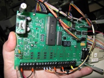
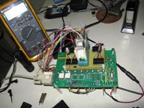
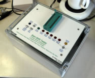
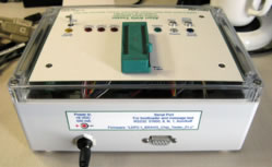
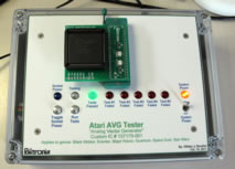
My stand-alone AVG Tester box is based on a Microchip PIC18 series microcontroller. The PCB is one that I designed about 15 years ago for another project. I just populated and programmed it for this new application. The serial port provides text messages out to a terminal program such as HyperTerminal running on the PC. The serial port also provides a bootloader function so I can reflash the PICmicro without opening the box. The tester performs many high speed tests on the AVG (plugged into the green ZIF socket). A green light indicates that all tests were passed. Any red light indicates a specific type of failure. The failure type is moot considering that a bad AVG chip is simply a bad AVG chip. The tester box can also loop the tests indefinitely and deliver an error count to the PC screen. This way, you can let an AVG chip run for hours or even days to test its endurance.
Top ---- Arcade List ---- Home
