
WG6100 Germanium Diode Discussion
Over the last few years, I have poured through all available schematics and parts lists trying to answer answer the question "Why are D807 and D808 in the P327 deflection board the germanium type?". I haven't determined yet exactly what part that was originally used, but I think I have a lot of info to offer.
Germanium diodes are very hard to source these days (but not impossible) and since there is no real advantage to installing them, I recommend installing the silicon 1N914 or 1N4148 devices in their place.
The original favorite application of Germanium diodes was in crystal radio sets as an AM detector. Since the forward bias currents were so tiny, ranging in microamperes, the forward voltage drop of the Ge diode was much lower than that of a silicon diode and thus it was easier to receive and demodulate radio broadcast signals. However, the forward voltage drop rises very quickly and significantly as the current increases restricting the advantage of low voltage drop to only very low current applications.
A common application of the 1N100A diode has been in clipping circuits. The Atari game Quantum has a few Ge diodes at positions CR3, CR4, and CR6. Parts CR3 and CR4 are connected at the outputs of the +/-15V regulators. It has been standard practice since the introduction of the 78xx ans 79xx regulators to use standard rectifier diodes in this application such as 1N4002 through 1N4007 or even the smaller 1N914 and 1N4148. Part CR6 is used at the input of a 74LS14 inverter gate that is also connected to the contacts of the reset switch. I am assuming that the diode in this position provides ESD protection by shunting transients to the +5V power rail. A zener diode connected across the switch (from the gate input to ground) would have done a better job although the zener diode would have to be of the TVS (transient voltage suppressor) type to be reliable. Standard 1/2W and 1W zener diodes can be permanently shorted by ESD events. Maybe another reason CR6 is there is to shunt small inductively induced transients away from the 74LS14 gate input. PCB traces are in fact inductors so this may have been common practice when Quantum was designed in 1983. Regardless, a simple 1N914 or 1N4148 diode would certainly had been sufficient. It is my belief that some design engineers learned about the uniquely low forward voltage drop of Ge diodes (maybe in theory in their first year of college/university) and didn't realize that this characteristic was easily overwhelmed and lost above a very low amount of current. Assuming that the Vf = 0.3V regardless, it becomes a common mistake to apply the Ge diode to power clipping or rectification circuits thinking that it would clamp the voltage closer to the nominal value than a silicon diode would. In fact, this is not the case. If this was in fact the intent, there are Schottky diodes that will maintain forward voltage drop values much lower than silicon diodes at significantly higher currents than any Ge diode ever could.
So for clipping applications such as Quantum, the 1N100 diode would be better to have been something like
BAT41: Digikey 497-2493-1-ND, Mouser: 511-BAT41
BAT46: Digikey 497-3768-1-ND, Mouser: 511-BAT46
About D807 & D808:
There were two different devices. One was a small glass axial case about 0.125" or 3mm long (commonly known as DO-35 and same as 1n914 or 1N4148). The other was about 0.3" or 6mm long (commonly known as DO-7). The DO-7 was typically orange with a yellow cathode band. The DO-35 was typically clear glass with orange at one end and a black cathode band. It was common to be able to see a small bonding wire inside it.
As far as I can tell, the smaller version of the diode was a 1N100. The larger one may have been similar or the same as the NTE110A.
1N100:
Datasheet: datasheetsite.com/1N110a.pdf
Source: americanmicrosemiconductor.com/1n100
Source: effectsconnection.com/1N100ANTE110A:
Datasheet: nte-electronics.com/nte110a
Source: mouser.com/nte110a
Source: newark.com/nte110a
What do D807 and D808 do?
The diodes D807 and D808 are part of the video input protection circuitry. That's right, the P327 had such a circuit built right in. Older versions of the deflection board had this circuitry added to it by mounting a daughterboard (about 1.5"x5") to the side of the PCB that is closest to the CRT. The P314 did not include this circuit.
Do not confuse this input protection circuit with the acclaimed LV2000 board. The LV2000 is also commonly referred to as an input protection board but it is actually a voltage regulator that takes care of the plus & minus DC power regulation circuitry and it has nothing to do with this discussion except that when a bad video input causes an excessive output current draw, the transistors (Q700, Q701, Q702) and a couple of resistors (in the same area of the pre-regulator stage) were severely stressed. This often led to failure of the DC supply. The LV2000 fixes this weakness but does nothing to limit the current drawn by the big TO-3 frame-mounted transistors. It does protect the DC regulation circuit.
The video input protection circuit consists of the following components:
The components C804, C805, R811, R810, form a filter. The purpose of this filter is to detect when an X or Y input goes active (as apposed to inactive which is zero volts) for an extended period of time. If an input does go active and stays that way long enough for C804 or C805 to charge up, this will turn on either Q804 or Q805 depending on the polarity of the input signal.
Once one of these transistor switches is thus enabled, the diodes D805 thru D808 jump into action. D805 & D806 work on the X channel. D807 and D808 work on the Y channel. When an input signal becomes excessively active and is essentially stuck on long enough to turn on Q804 or Q805, one of diodes in the effected pair conducts signal current away from the input of the respective deflection preamplifier, thus dramatically limiting the output current conducted by the final stage, the frame-mounted TO-3 transistors. Due to the time delay function of the first part of the protection circuit described previously, short duration peaks of the input signals are not clipped and so operation will be normal. Only when an input goes highly active for too long does it get clipped. This active current limiting method is obviously much faster than blowing a hard fuse, is infinitely repeatable, and will also quickly recover when the bad signal goes away.
Okay, so what's with the germanium diodes?
All I can do here is guess. The "Y" amplifier has a little bit more current gain than the "X" (assuming that "Y" is the long dimension of the CRT). For a given video input voltage, it will conduct more current. It is commonly understood that a germanium diode starts to conduct around 0.3V and a silicon diode starts to conduct around 0.7V. Since D807 & D808 are used to clamp the "Y" channel and since they are germanium, they will begin to conduct at a lower voltage than the silicon pair D805 & D806 on the "X" channel. Also, because R811 is half the value of R810, the "Y" filter circuit will charge faster and turn on sooner than the "X" counterpart.
So what will happen if you install 1N914 or 1N4148 diodes in place of D807 & D808?
All this will do is raise the final peak output current of the "Y" channel a little bit in the event that the "Y" gets stuck on. This is not really a problem for a few reasons…
In the end, I don't think that it's worth the effort to source and install germanium diodes in locations D807 and D808. A standard 1N4148 or 1N914 will do just fine.
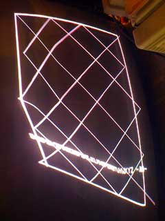
This is what the picture will look like when D807 or D808 are bad...
Go to: .......Top .......Back to Parts List....... Bill's Classic Arcade ....... Home