
mirrored from: http://home.t-online.de/home/stephan.hans/tricks.htm
(last update: 24.02.1999)
Project # 1: DUAL-KEYBOARD Circuit
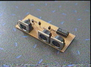
PHOTO / prototype:
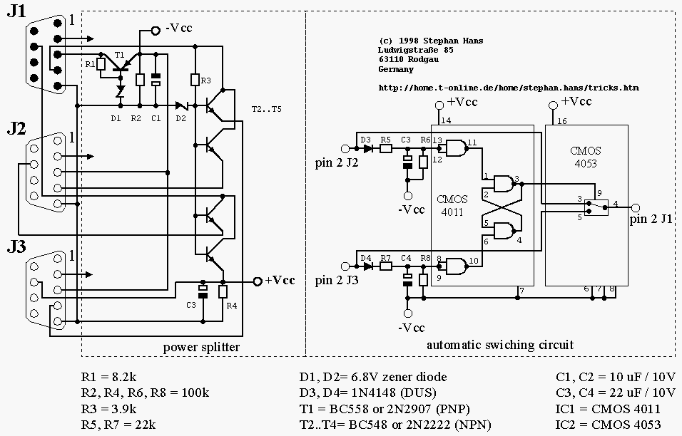
Sheet:
How it works:
The pc remains able to communicate with the keyboard 1 by pulling down its data line (pin 2 of the DIN connector) using diode D1. When one of the keyboards communicates with the pc, the data line is pulled to low (with the start bit) by the corresponding keyboard. This is detected by T1 and T3. Via T2 and T4 the cmos switch 4053 is triggered and pulls the clock line (pin 1 of the DIN connector) of the other keyboard to low. So the other keyboard buffers its data until the clock goes high again, this time depends on the combination of C1/R2 and C2/R4 and must be long enough for that the first keyboard is ready with sending its data.
By the way, with two transistors, two resistors, one capacity and 6 diodes more, the whole thing could be extended to work with 3 keyboards (the cmos circuit 4053 contains already 3 switches).

Updated: 
Thanks to all of them who responded to my circuit here are some answers to the frequently asked questions:
Some explanations (for those guys who never
heard of nanofarads):
| Picofarad: | 1 pF | 10 E-12 Farad |
| Nanofarad: | 1 nF = 1000 pF | 10 E-09 Farad |
| Microfarad: | 1 uF = 1000 nF | 10 E-06 Farad |
Some hints for the transistors:
Instead of the BC548 you can use nearly every n-type bipolar transistor (e.g.
2N2222 or 2N3904) and
instead of the BC558 you can use nearly every p-type bipolar transistor (e.g.
2N2907 or 2N3906).
Something about the R/C part in my circuit:
As you can see, C1 and R2 (and C2 / R4) form a small timer. During the time
determined by one of these pairs, the circuit is blocking the "other"
keyboard while the "one" is transmitting its data. I've choosen the
values for C1/C2 as 22 nF and for R2/R4 as 47 kOhm (47 000 Ohm). Because the
timing factor depends on the product of both, you can also take 100 nF and 10
kOhm instead of it. But don't choose the value of the capacitor to high, because
the transistor has to shorten its charged power.
And now to all of them who wanted to use PS/2 connectors
instead of the 5 pin DIN connectors:
Sure it's possible, but take care of the different pinout for
the PS/2 connectors:
|
|
| Remember:
at the 5 pin DIN connector, the pins are named: |
| 1 | clock |
| 2 | data |
| 3 | no connection |
| 4 |
GND |
| 5 | +5V |
And now for them who have begged me to show some
more pictures of the prototype, especially the "layout" side, here
they are, but don't complain if it's too confusing (so be warned):
(By the way, don't bother about the two LEDs that I used for "control"
purposes)
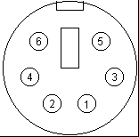
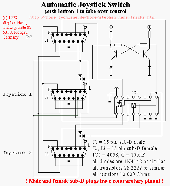
Project # 2: AUTOMATIC JOYSTICK SWITCH
(by popular demand)
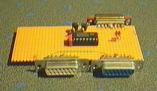
prototype:
Project # 3: Automatic switch for two serial mices (or trackball, or spinner, or touchpad.....)
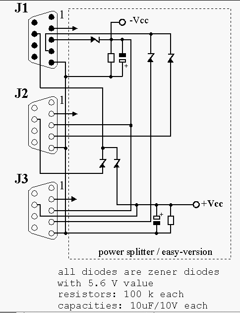
If you would say the power splitter is rather complicated, you're right. It's only because I've had no more zener diodes but plenty of transistors (btw: for me a transistor is even cheaper than zener diodes). Now here's a proposal for a much easier power splitter, which should work instead of the "complicated" one (haven't tested it 'til now):
Project # 4: SUPERDUPERARCADEJOYSTICKCONSOLE
Now, lets go on with the arcade console:
|
1 |
2 |
3 |
4 |
5 |
6 |
7 |
8 |
|
|
1 |
Alt |
|||||||
|
2 |
Str (l) |
|||||||
|
3 |
Shift (l) |
|||||||
|
4 |
A |
Capslock |
Q |
TAB |
^ |
1 |
< |
Y |
|
5 |
D |
S |
E |
W |
2 |
3 |
X |
C |
|
6 |
ESC |
F2 |
F4 |
F6 |
F8 |
F10 |
F12 |
Space |
|
7 |
F1 |
F3 |
F5 |
F7 |
F9 |
F11 |
Druck |
Down |
|
8 |
G |
F |
T |
R |
4 |
5 |
V |
B |
|
9 |
J |
H |
U |
Z |
6 |
7 |
N |
Rollen |
|
10 |
L |
K |
O |
I |
8 |
9 |
M |
, |
|
11 |
� |
� |
� |
P |
0 |
� |
. |
- |
|
12 |
Enter |
# |
+ |
� |
Left |
|||
|
13 |
Ende |
Entf |
Backspace |
Einfg |
Up |
Pause |
||
|
14 |
4 (#) |
7 (#) |
PageDown |
Pos1 |
PageUp |
1 (#) |
Right |
|
|
15 |
Shift (r) |
|||||||
|
16 |
Str (r) |
|||||||
|
17 |
6 (#) |
5 (#) |
9 (#) |
8 (#) |
Numlock |
/ (#) |
2 (#) |
3 (#) |
|
18 |
, (#) |
Enter (#) |
+ (#) |
* (#) |
- (#) |
0 (#) |
||
|
19 |
AltGr |
A few words about the
"ghost-key" problem:
If you press 3 buttons which are at the edges of a rectangle in the keyboardmatrix,
for example the keys:
<F8>, <F10> and <5> you can't detect with a matrix if
the key <4> is pressed or not, so the keyboard controler generates
a "ghost 4" and send it to the pc. And furthermore, if you have
all keys at the edges pressed and you release one of the keys, nothing happens
(no keyrelease-code would be send to the pc) cause the keyboard-controler
in fact did'nt notice that one of the keys is released.
So you have to be careful which points in the keyboardmatrix you will use
for your controls. Such keys like <1>,<2> and <3> wont
cause any problems because they are only used for "game selection"
purposes. But when it comes to action, there should be no interference between
the controls used.
Updated:
How to eliminate the ghost-key problem (thanks to George for the hint):
If you connect a standard diode in
serial to each button, the ghost key problem vanishes from the electrical
point of view. Check out, in which "direction" the diode could
be inserted at your gutted keyboard (it depends on whether the keyboard
manufacturer uses "running zeroes" or "running ones"
to scan the matrix):
|
|
|
|
"running zeroes" |
"running ones" |
I haven't checked it out 'til now,
but it should work in theory.
OK. that's it for now. I'll make some pictures when the "mechanical"
part is ready. (It's still not
ready ;-( )
Stephan
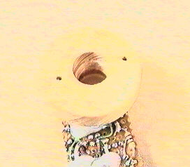
Project # 5: SPINNER for superduperarcadeconsole
Hi folks, my spinner device is ready:
|
|
|
|
Superduper spinner with stroboskop pattern visible |
Superduper spinner / sideview |
|
|
|
|
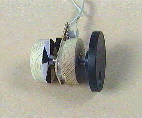
From left to right: knob,
steel axis, wooden disk with |
Sensor board assembled on
the wooden disk. |
|
|
here the 13mm hole with
the 11.5mm core |
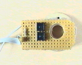
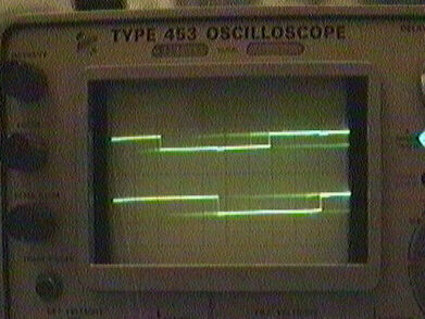
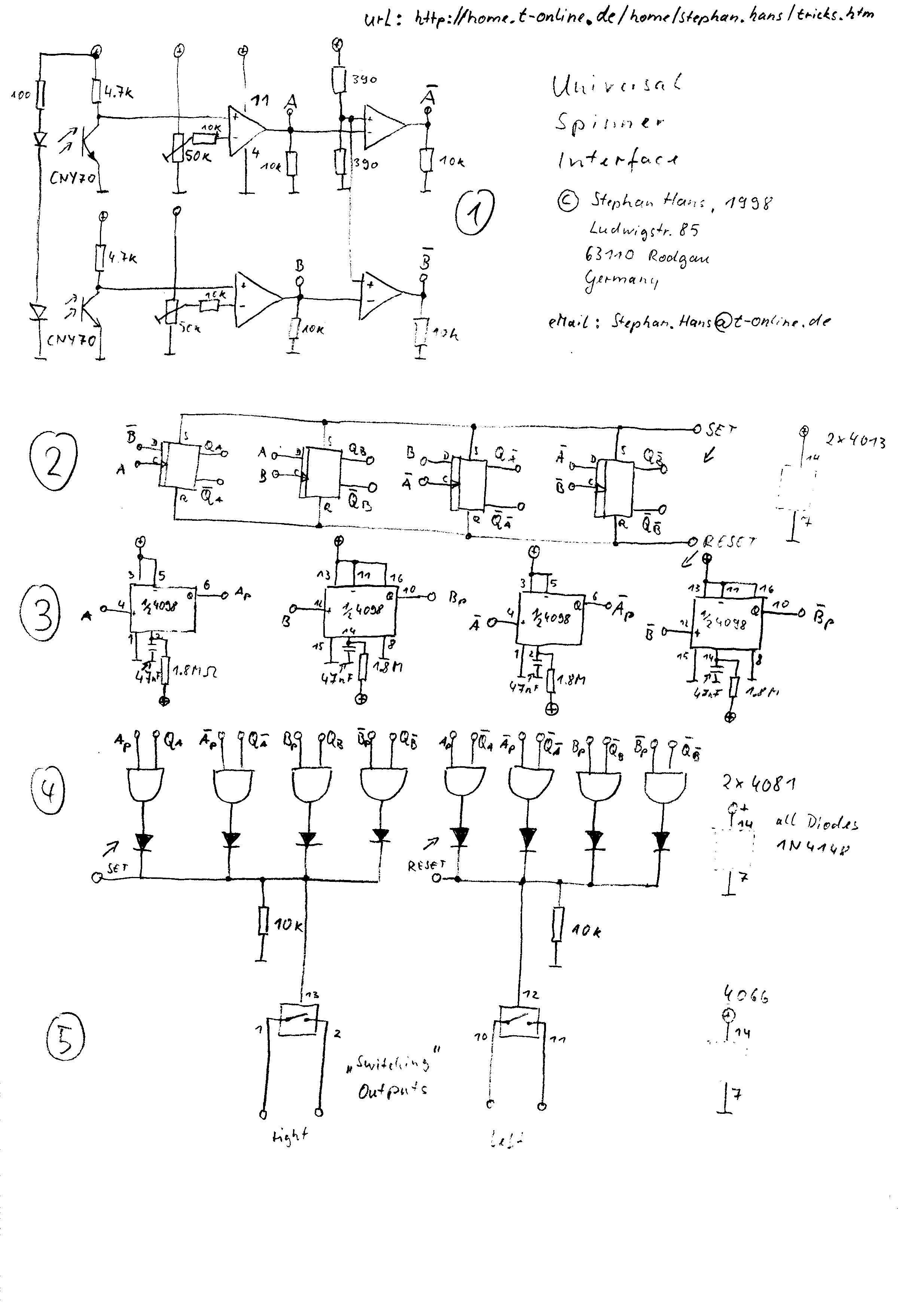
Project # 6: universal spinner interface for keyboard, joystick or gamepad
Hello arcade freaks, my universal spinner interface is ready now:
First an introduction into the gray code which is usually
used for rotary devices:
The signals A and B represent the signals which were delivered by the photo-transitors
(after amplification)
|
|
It is possible to change the motion direction whenever you want. And you
can see that you can always determine the direction of movement if you know
the last state! So it's nescessary to store this state in some way.
Now for something completely different,
the larch.... oh no, the verbal circuit-description:
First stage of the circuit is a 4 times OpAmp (TL084) which amplifies the signals from the photo-reflex sensors (signals A and B). Two of the OpAmps just act as inverters to get the inverted signals A* and B*.
The second stage of the circuit consists of 4 D-flip-flops (2* 4013). There the "direction" is going to be stored. The flip-flops are triggered (positive edge) by the signals A, B, A* and B* while the D-inputs are connected to B*, A, B and A* so you always have for the right direction the Q-output set (QA, QB, QA*, QB*) and for the left direction the Q*-output (Q*A, Q*B, Q*A*, Q*B*). Btw, all the "set" inputs are tied together and all the "reset" inputs are tied together, they will be connected to the outputs of the fourth stage.
The third stage:
With four monoflops (2* 4098 or 4528 or 4538) a pulse signal for each possible transition in the gray-code is generated. So we have a Ap, A*p, Bp and B*p pulse. I've designed the pulse duration time by 17ms. In fact I used a 47nF capacity and a 1.8 MOhm resistor.
The fourth stage:
The pulse outputs are combined via 8 AND gates (2* 4081) to the direction outputs of the flip-flops. (Ap AND QA, A*p AND QA*, Bp AND QB, B*p AND QB* for the "right" direction and Ap AND Q*A, A*p AND Q*A*, Bp AND Q*B, B*p AND Q*B* for the "left" direction).
Each output for one direction is tied via a diode (Anode at output) to a single 10 kOhm resistor which is then tied to ground (2* (4 diodes, 1 resistor)). In fact these diodes simple simulate two OR gates with 4 inputs.
Let me name the outputs of this stage as "right-pulse" and "left-pulse".
The fifth stage:
Is just a CMOS switch (4066 or 4016, only two of the 4 available switches are used) where the steering inputs are connected to right-pulse and left-pulse.
(In the prototype shown above, I use the remaining switches to drive two LEDs, so I can survey the proper function of the circuit)
Oh, not to forget: the "set" inputs from the D-flip-flops are connected to "right-pulse" and the "reset" inputs to "left-pulse" too.
Now the outputs of the two CMOS-switches could be used to shorten a keyboard-key or a joystick-button or a gamepad-pad....
Note that the ground and the supply voltage level (+5 V) of the interface should be the same as for the driven device (otherwise you can damage the switches within the 4066). The easiest way to achieve this, is to supply the interface by the keyboard or joystick port.
I think the circuit is nothing for beginners ! When I write the sheet down to paper, I'll scan it and put it at my site. Maybe someone will find the time to "write it down" with a CAD-program.
Update 02.04.98: click here for the scanned sheet.
Very experienced electronic freaks should be able to build the circuit following to the verbal description (availability of CMOS-databook assumed).I just checked out the interface and connected the circuit to my (second) cherry keyboard controller.
IT REALLY ROCKS !
I tried out ANNOID (the arkanoid emulator) and it worked "like a charm".
I'm ready now for arkanoid within mame v0.31,
hope the mame team will be ready soon !
(really can't wait any longer.....)


