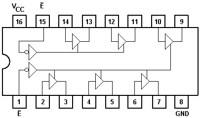
Note the 74LS367 has 2 sections with 2 seperate enables !
{Insert picture of probe here}
A Logic Probe is one of the basic troubleshooting tools for common electronic logic circuits (TTL circuits, chips with the 74XX pre-fixes). Almost all video game circuit boards are built using TTL chips. These chips will occasionally fail and the Logic Probe is a tool that affords us a look into what may be failing. Logic probes are fairly inexpensive about $30.00 from Jameco, Radio Shack (Hurry up RS is closing these out now 5/03!) or the like. Logic probes have their shortcomings too...
Logic Probes have 3 LED's and some have a Piezo buzzer. The 3 LED's indicate...
RED
High logic state a binary 1. TTL chips consider +2.4 to +5 VDC to
be high.
GREEN Low logic state a binary
0 TTL chips consider 0 to + 0.8 VDC to be low.
YELLOW Pulsing state
(yellow &/or piezo buzzer)
Your actual LED colors may vary depending on make!
Notice the voltage range between +0.8 and +2.4
is undefined. Any steady voltage state in this undefined range should
not light any LED's on the logic probe & is indicative of a problem
such as overloaded/ weak output or missing pull-up resistor.
Transistor Transistor Logic is the commonly
used format of logic chips on PCB from the mid 70's to present day.
These chips may be identified by the numbers printed on their top.
74XX Standard TTL family
54XX Military Grade TTL, made to higher standards
against radiation, moisture & failure.
93XX Early TTL family.
The TTL family has been improved over the years in speed & performance. These newer sub classes are identified by modifiers such as....
74LSXX Low Power Schoktty Type
74FXX Fast
74SXX Schoktty Type
74HCXX High Speed CMOS Type
All chips perform the same logic operations, a 7400 Quad 2 input NAND gate will perform the same as a 74LS00 but there is minute improvements in Propagation (speed at which the signal travels through the gate) and actual power consumption by the individual chip.
When replacing a TTL chip you should strive
to match the original chip. It is acceptable to replace a 74XX with
a newer class 74LSXX but you should avoid retreating back down the ladder
of evolution and replace a 74FXX chip with a 74XX for example (in this
case you are replacing a high speed chip with a slow speed chip & inviting
problems).
40XX or
45XX
Complimentary Metal Oxide Semiconductors. This logic family is a step beyond the TTL family. It's most notable feature is that it can operate at much higher voltages (over +12 VDC) than a TTL and that it is ANALOG in it's performance compared to the DIGITAL nature of TTL. TTL's are considered digital as they have only 2 valid states Low (0) and High (1). CMOS have states that are proportional in nature. For example if you had a 4069 Hex Inverter, with a functional (not necessarily pin out compatible) equivalent of 7404; we know that in a 7404 a given gate input state of High (1) then it's output would be inverted or Low (0). The 4069 would be different, first it's input state could be a voltage range from 0 to the operating voltage, say in this example +12 VDC. If the input voltage for a given gate was +4.0 VDC then the output would be +8.0 VDC or the inverse proportion of the input relative to the operating voltage.
CMOS is useful for handling audio outputs (like on Pac-Man using the 4066 at 1N) or creative people have even used them to do quickie video inversion on Nintendo games for the color section.
It is possible to use a Logic Probe to troubleshoot
CMOS chips if the probe is designed to handle CMOS. Most probes have
a switch to toggle between CMOS and TTL chips.
Well now is when schematics become important.
Schematics are the road map for the logic signals that are traveling around
the PCB.
Most schematics will have labels marked on
them such as RESET (Imagine that the line
is drawn above the word RESET and not through it, HTML does not support
a bar over characters yet). The line over the word RESET requires
us to read it as "RESET NOT". This method also indicates what state
it is, normally the PCB trace that contains the signal RESET
is High, (1) or +2.4 VDC or greater. When the event is active, the
Pac-Man board decides it is time to perform a reset then this PCB trace
will go Low and initiate a reset function. The RESET
is called a active low signal meaning that the reset function is activated
when the line goes low.
Schematic labels do not follow strict naming conventions. Chips sometimes will be marked as for inputs and outputs. The letter Q always indicates an output.
Schematics may also have arrows on given traces, this is to indicate the flow of the signal, if it is a input or output to your given chip. Generally schematics are organized so that the flow of a signal follows a logical convention. Inputs generally enter the circuit from the left or top and the outputs exit from the bottom or right sides. Signal processing generally is shown to proceed from left to right and top to bottom on schematics.
Now would be a good time to learn a bit more of the ins and outs of these chips. The TTL Cookbook by Don Lancaster will provide you with some insight into what actually is going on inside of these chips. ECG & NTE, both replacement chip suppliers, offer catalogs that include descriptions and pin out diagrams. Any of these sources or even manufactures' data books will give you some idea of which pins are inputs and outputs.
Online several chip manufactures have their
data books, my personal favorite at the moment is Fairchild (www.fairchildsemi.com).
Texas Instruments just recently sent out "freebie" pocket reference books
with a listing of most common TTL, pinouts, truth tables etc. Worth
getting but it has an error on 74LS157!
Okay, so grab your probe & schematics.
Since you have already checked the Pac-Man board for voltage clip your
logic probe leads to a power source, I like using C2 or C3 both are moderate
size electrolytic capacitors (470 mfd at 16VDC) and are marked as to which
end is positive/ negative. C2 is central to the PCB. (If
you are working on something else you may want to just use a rail filter
cap, most Printed Circuit Boards have the TTL chips arranged in rows and
columns, columns go up & down and are flanked by power rails with Ground
being the opposite end of pin 1 and Voltage (+5 VDC or VCC) being at the
same end as pin 1. Each of these rails usually will have a small
"spike filter" capacitor across them where you can attach your logic probe
to power.)
Now test your probe by touching the tip to the positive side of C2. You should have a solid, steady {RED} LED indicating high (some probes will also have a tone). Your board is powered up right?
Next probe the negative side of C2, solid steady {GREEN} LED indicating low state.
Let us see if that RESET line
is working. Probe the RESET line at the Z80 @ 6B
pin 26 (or the test connector pin 35 or the 74LS02 @ 7L pin 13 or the 74LS259
@ 8K pin 15 or the PCB edge connector pin 6).
Your probe should indicate a High state, {RED} LED.
Hold your probe in place, watch the LED's and
press the red button on the Pac-Man board (SW1). You should notice
the {GREEN} LED light as RESET is activated by the low
state you just witnessed & the entire game will reset and cycle through
the startup test routine as if you had just turned the game on.
Notice that there is also a RESET signal shown
on the schematics between the 74LS161 @ 9C pin 15 and the 74LS02 @ 7L pin
12. RESET is the opposite state of RESET and would
act opposite of the states you just observed previously.
WHAT not working?? Hmmmm, if
your game is infact running but the red SW1 has no effect, test your SW1
first ~ probe the 74LS161 @ 9C pin 9. This should be high & go
low as you depress SW1, if it doesn't go low, back track to the switch
& test again for a high state that goes low. If it works at the
Switch but not at the chip at 9C then look for a break in the trace between
the two points. If it does not work at the switch then try using
a jumper wire attached the the PCB ground (same as the logic probe ground
point) and quickly touch 9C pin 9. If all works now, suspect your
switch. If not, suspect the 74LS161 @ 9C. You can hold your
logic probe to 9C pin 9 and touch the ground jumper wire to the logic probe
tip if you want to observe the state change.


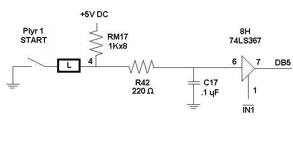
You can use the same technique as above to troubleshoot input switches such as the joystick, start buttons, Coin inputs or even the Dip Switches. You will notice that all of these switches have pull-up resistors. A pull up resistor brings the voltage up to +5 VDC so that the inputs are at a normally High state (1). On Pac-Man the pull-up resistors are RM6 (Dips), RM7 (test/table/start/player 2 controls), and RM8 (coin, credit, player 1 controls). The RM is a designation for Resistor Network or Resistor Array. You will notice above that RM7 is described as a 1K x 8 (1 K by 8), meaning that this resistor array has 8 resistors of 1K ohm value with a common lead.
You will also see a small .1 micro Farad capacitor (C17) tied to ground, this is to lengthen the momentary pulse (a low state as the switch is closed connecting it to Ground) as the capacitor recharges and enable the logic to actually have enough time to register a input. This also acts as a "debounce circuit" eliminating the circuit from registering many switch closures and opens that occur in the tiny time window as the switch changes state. (Notice the Dip Switches don't use these capacitors).
You can "see" the controls/ dips at work with your logic probe from the switch. Place your logic probe at the 74LS367 (Hex Buffer Tri-State) 8H pin 6. It will be normally High until you press the player 1 START down, when it will change to Low. So if I look at the output of this circuit, I'll see the same thing at 8H pin 7 right? WRONG. Notice the output is labeled DB5 (Data Bus 5), but DB5 is also at 8E pin 7, 8D pin 5, 3F pin 6, 4D pin 7, and 6D pin 6. We're on the BUS here man! Not only is this now the path for information about the joystick being pressed down but it could also be a Player 1 Down, or Dip 5 or info to the Graphic ROM's or Sound Section etc... The BUS is the pathway for data to travel in either direction. In our case the Data BUS is 8 BITs wide, our joystick closure is only one bit of information in a system that can directly access 64K bits.
So how do we keep up with this information? The same way the post
office delivers your mail, you have a address that is explicitly defined
to you. Okay, what's the address for "Player 1 Start"? We'll
save that for latter. For now it is important to notice that if you
are on the bus, things will be going too fast to see what you want.
If you notice the 74LS367 chip at 8H has a line at pin 1 IN1
which is an input (see the arrow pointing to our chip?). This is
used to ADDRESS our chip 8H and tell it "Hey man, what data do you have
for me on DB4~DB7" (it also reads DB0~ DB3 from 8F concurrently) at which
time the Central Processor Unit (CPU) is only looking at these particular
inputs at this given address, which includes our switch Player 1 START.
So things are too fast for us to know if they are working properly on the
BUS side but we can check to see if they are working properly before the
Hex Buffer and we can also be sly & check to see that the Hex Buffer
is being used by the CPU if we look at the IN1 signal
at pin 1, it must go LOW to enable a read from chip 8H.
The Clock Circuit is the primary time keeper
for the circuit board, much as a drummer is for a band. Pac-Man uses
a single crystal to provide the timing for the Z80 and develop the Video
synchronization signals for the monitor output.
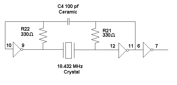
The logic probe will not test a crystal properly (overload it's output)
so check the output of 8B pin 7 for a pulse. Note the enable lines
of the 74LS368 @ 8B must have pins 1 & 15 low at all times to work.
If you do not have an output at 8B pin 7 suspect the crystal.
Okay, let's find a pulse...... Upper left corner of your schematics for Pac-Man is the CLOCK circuit. You will see 3 signals listed here.....
6 MHZ
6 M*
6 M*
Probe chip 8B pin 13. All three LED's should light and your probe should purr at a fairly high speed. (It is important that both High & Low LED's light, if one is missing this could indicate a chip that is not fulfilling the requirements of TTL logic and may cause problems down the line, spent many a hour troubleshooting a Xenon pinball board because I overlooked this....)
If you are adventuresome you can follow the
6MHZ signal through the divider circuit at 8C, 3R, 3S. Here
the signal is divided down to produce the VIDEO SYNC signals for the monitor.
Follow the 16H, 32H, 64H and 256H to 2P, 3P and eventually
out to 5N pin 11 where we have CMPSYNC.
'The logic probe can find many problems very quickly & it doesn't take long for you to mem(orize) chip outputs,e.g., quite common in older boards are the 74161 series that output at 11/12/13/14 and the popular 74157 series that output at 4/7/9/12. I always check outputs & if I find one bad, I drop back to the inputs & if they are ok...time to change the chip.
You can detect more complex troubles after getting used to using a logic
probe & knowing what to expect, e.g., 74161 outputs starting at pin
11 & listening to the pulse tone & looking at the LED flashes,
you learn to expect a doubling of that when moving to pin 12, and again
to pin 13, and once more to pin 14. If at some point, you fail to hear
this or it sounds the same on 2 adjacent pins, you know to further investigate
this chip." Bob Roberts
So far we know how to check for RESET,
in order for our game to run we know this line must be high. If the
line is pulsing then we have a condition where the "watchdog is barking".
Watchdog circuit acts like any good watchdog, it observes the PCB (Pac-Man)
in action by monitoring a select few ADDRESS Lines for activity.
Lack of activity within a preset number of machine cycles will alert the
watchdog that something is wrong. Like all good watchdogs, he "barks"
or send a signal out on the RESET line (74LS161 @ 9C pin 15) that forces
the CPU to restart over as if the power had been turned off.
What makes the watchdog bark?
Basically the CPU is hung in a loop, confused for some reason be it
BUT FIRST, we must be sure that we have all of the correct timing signals that the watchdog timer uses to count down to a "bark".
Assuming that you have worked through the Sync generation section above (8C, 3R, 3S, 2P, 5M, 2R, 2S) with good results. Next check VBLANK for a pulse at the 74LS161 @ 9C pin 2. Missing a pulsing VBLANK ? Go to the 74LS10 at 3P, pins 8, 9, 10, 11 then to the 74LS74 at 5M pins 2, 3, 5, 6 (be sure pins 1 & 4 are pulled high).
The 74LS161 will generate the "bark" or watchdog reset signal that will
send a pulse to the RESET line then on through the 74LS02 @ 7L where
it becomes the RESET line to the Z80 pin 26.
Also know as Logic Tables. These list the input & output
conditions for a gate or circuit. If you picked up a TTL Cookbook
or the like you will have examples of these. Depending on your drive
to learn all the inner workings of digital logic you may decide to memorize
all the gates and their functions. All are math based (AND, OR, NOR,
INVERTING etc...) so it will be fairly easy once you associate the symbol
with it's name.
Truth tables can also be constructed for larger circuits or in our case the entire Pac-Man board. Done on a chip by chip, pin by pin level at given conditions, say intermission or Game Over Demo. Each pin will have a listing of.....
P.....yellow pulse like xtal
LP....low pulse
HP....high pulse
HLP...high to low pulsing
L-above for a situation where an output (in attract) is low
for 20 to 30 seconds and then does one of the above & recycles.
H-& above
L....low
H....high
Bob Roberts suggested these and it is a great idea (now if someone could
just create the entire series and post it here for us!).
A logic pulser may seem like a wise addition to your troubleshooting tools. Also called a signal injector, it appears similar to a logic probe and is used in conjunction with a logic probe. A logic pulsers' purpose is to generate a pulse (usually 5 Hz or so) to input into a circuit that you are monitoring with your logic probe. 5Hz is a relatively low rate that is easy to see with the probe. It is a bit tidier and safer than a jumper wire to ground as we used early in troubleshooting SW1.
Many techs do most of their troubleshooting with a logic probe, it is
quick & easy. It helps find open circuits, short circuits &
stuck states. It is a good start
.
"This is far & away, the cheapest & easiest way for a collector
to T-shoot a board, once the basic skills are captured." The
Real Bob Roberts
Created 12/29/98
Updated 5/06/03
![]()
Note that you cannot click on the e-mail address you must type it in
(Spam is horrible now), please also include "PAC-MAN" in your subject line
to help me sort the garbage out.